- CR Home
- CR Group
- 中文版

 Introduction of Flip Chip Technology
●Traditional packaging technologies normally make the active side of the chip face upside, and its back faces to substrate or frame for mounting and bonding; while Flip Chip packaging technology( see figure 1) makes the active side of the chip face towards substrate or frame, to realize interconnection between the chip and the substrate via the soldering salient points on the chip which is in array arrangement.The common salient point structure mainly includes the two types of solder ball and copper pillar.

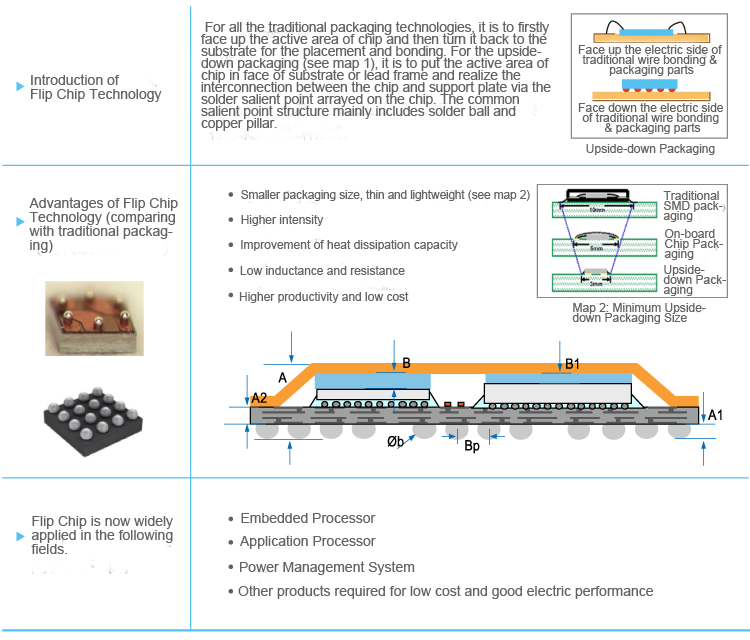
Advantages of Flip Chip Technology (compared with traditional packaging)
●Smaller packaging size, thinner and lighter weight (see figure 2)
●Higher intensity
●Improvement of heat dissipation capacity
●Low inductance and resistance
●Higher productivity and low cost
Flip chipis now widely applied in the following fields.
●Embedded Processor
●Application Processor
●Power Management System
●Other products required for low cost and good electric performance
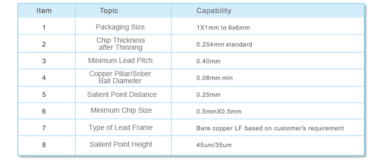
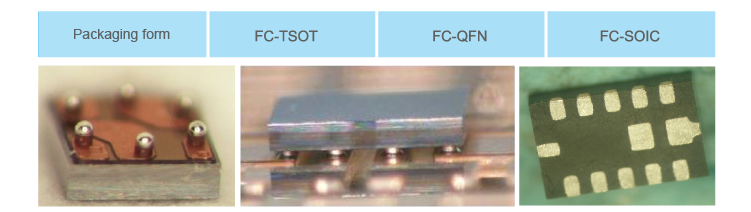
Process Capability for Anst's Flip Chip
●Now, Anst can provide full series of packaging technologies including copper pillar and solder ball type of Flip Chip on lead frame (interconnection of chip and lead frame)
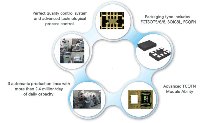
●Process Capability